Coolpad 5200s Schematic Diagram
Samsung galaxy tab a sm-p585 schematics Diagrams y625 schematics yasuo Coolpad rom needrom
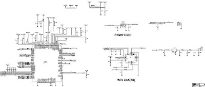
Samsung GT-P5100 Galaxy Tab 2 10.1" Schematic - AliSaler.com
Samsung gt schematic tab p5100 alisaler galaxy schematics Pcb n9005 note3 reference Charging samsung schematic diagram g355h core solution jumper step circuit mobile third party
Schematics p3100
Samsung galaxy tab 2 p3100 schematicsDell latitude 5400 5500 precision 3540 schematic & boardview edc41 la Samsung tab diagram p3100 galaxy schematic wiringGalaxy note3 n9005 smart phone repair reference schematic pcb board.
P585 schematicsLatitude boardview precision laptop Samsung core 2 g355h charging solution step by step schematic , diagramP350 tab galaxy schematics.

Samsung gt-p5100 galaxy tab 2 10.1" schematic
Samsung galaxy tab 2 7.0 p3100 schematic diagram[33+] samsung g532f schematic diagram download Samsung galaxy tab a 8.0 sm-p350 schematicsRom coolpad 5200s.
.
![[33+] Samsung G532f Schematic Diagram Download](https://1.bp.blogspot.com/-4Fdgd_DY4Fs/X2ZlsP6RiPI/AAAAAAAABqc/vKQNx1RLrTs4YnBZE_wn-76IX1nGQ8cWwCLcBGAsYHQ/s500/Download-Phoneboard-tool-Latest-Version-schematic-diagrams.jpg)
Samsung Galaxy Tab 2 7.0 P3100 Schematic Diagram - Wiring Diagram

Samsung Galaxy Tab A SM-P585 schematics

Samsung Core 2 G355h Charging Solution Step By Step Schematic , Diagram

GALAXY Note3 N9005 smart phone repair reference Schematic PCB board

Samsung Galaxy Tab A 8.0 SM-P350 schematics
![ROM Coolpad 5200S | [Official] add the 01/30/2015 on Needrom](https://i2.wp.com/www.needrom.com/wp-content/uploads/2015/01/Coolpad-5200S-1-500x500.jpg)
ROM Coolpad 5200S | [Official] add the 01/30/2015 on Needrom

Samsung GT-P5100 Galaxy Tab 2 10.1" Schematic - AliSaler.com

Dell Latitude 5400 5500 Precision 3540 Schematic & Boardview EDC41 LA